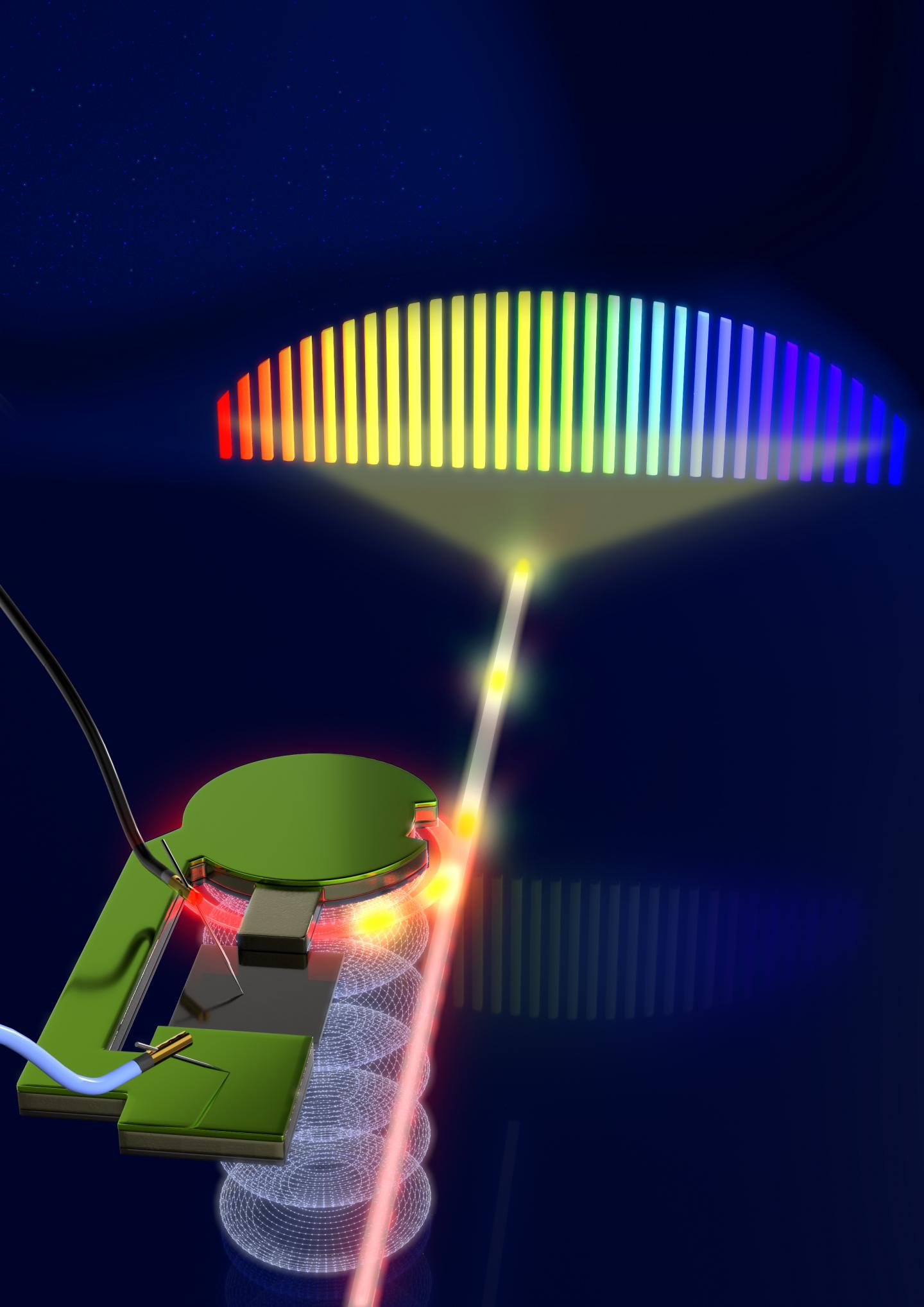
IMAGE: New technology uses acoustics to better control a pulse of laser light split into a frequency comb, potentially helping lidar to achieve detection of nearby high-speed objects.
view more
Credit: WoogieWorks graphic/Alex Mehler
WEST LAFAYETTE, Ind. — A self-driving car has a hard time recognizing the difference between a toddler and a brown bag that suddenly appears into view because of limitations in how it senses objects using lidar.
The autonomous vehicle industry is exploring “frequency modulated continuous wave” (FMCW) lidar to solve this problem. Researchers have built a way that this type of lidar could achieve higher-resolution detection of nearby fast-moving objects through mechanical control and modulation of light on a silicon chip.
The work, published in Nature, was conducted by the OxideMEMS lab at Purdue University and the Laboratory of Photonics and Quantum Measurements at École polytechnique fédérale de Lausanne (EPFL), a research institute and university in Lausanne, Switzerland.
FMCW lidar detects objects by scanning laser light from the top of an autonomous vehicle. A single laser beam splits into a comb of other wavelengths, called a microcomb, to scan an area. Light bounces off of an object and goes to the detector through an optical isolator or circulator, which ensures all reflected light ends up at the detector array.
What Purdue and EPFL researchers developed uses acoustic waves to enable faster tuning of these components, which could bring higher-resolution FMCW lidar detection of nearby objects.
The technology integrates microelectromechanical systems (MEMS) transducers made of aluminum nitride to modulate the microcomb at high frequencies ranging from megahertz to gigahertz. The optical isolator that the team developed as part of this process is further described in a paper published in Nature Communications.
An array of phased MEMS transducers, also used in cellphones to discern cellular bands, stirs light at gigahertz frequencies by launching a corkscrew-like stress wave into a silicon chip.
“The stirring motion modulates light such that it can only travel in one direction,” said Sunil Bhave, a Purdue professor of electrical and computer engineering.
Hao Tian, a Purdue Ph.D. candidate in electrical and computer engineering, built the MEMS transducers at the Scifres Nanofabrication Facility of Purdue’s Birck Nanotechnology Center in Discovery Park. He integrated the transducers with a silicon nitride photonics wafer developed at EPFL.
“The tight vertical confinement of the bulk acoustic waves prevents cross-talk and allows for close placement of the actuators,” Tian said.
Other transducers in the same technology excite an acoustic wave that shakes the chip at megahertz frequencies, demonstrating sub-microsecond control and tuning of the laser pulse microcomb or soliton.
“This achievement, bridging integrated photonics, MEMS engineering and nonlinear optics, represents a new milestone for the emerging chip-based microcomb technology,” said Junqiu Liu, the first author on the Nature paper who leads the fabrication of silicon nitride photonics chips at the EPFL Center of MicroNanoTechnology.
This light modulation technique not only integrates mechanics with optics, but also the fabrication processes involved, making the technology more commercially viable, the researchers said. The MEMS transducers are simply fabricated on top of the silicon nitride photonics wafer with minimal processing.
“As yet unforeseen applications will follow up across multiple communities,” said Tobias Kippenberg, a professor of physics at EPFL. “It’s been shown time and again that hybrid systems can obtain advantages and functionality beyond those attained with individual constituents.”
According to the researchers, the new technology could provide the impetus for microcomb applications in power-critical systems such as in space, data centers and portable atomic clocks, or in extreme environments such as those with cryogenic temperatures.
“Our results would not have been possible without this multidisciplinary and intercontinental collaboration,” Bhave said.
###
The work at Purdue is funded by the Defense Advanced Research Projects Agency and the National Science Foundation.
ABSTRACTS
Monolithic piezoelectric control of soliton microcombs
Junqiu Liu,1 Hao Tian,2 Erwan Lucas,1 Arslan S. Raja,1 Grigory Lihachev,1 Rui Ning Wang,1 Jijun He,1 Tianyi Liu,1 Miles H. Anderson,1 Wenle Weng,1
Sunil A. Bhave,2 and Tobias J. Kippenberg1
1Laboratory of Photonics and Quantum Measurements, Swiss Federal Institute of Technology Lausanne (EPFL), CH-1015 Lausanne, Switzerland
2 OxideMEMS Lab, Purdue University, 47907 West Lafayette, IN, USA
DOI: 10.1038/s41586-020-2465-8
High-speed actuation of laser frequency is critical in applications using lasers and frequency combs, and is a prerequisite for phase locking, frequency stabilization and stability transfer among optical carriers. For example, high-bandwidth feedback control of frequency combs is used in optical-frequency synthesis, frequency division and optical clocks. Soliton microcombs have emerged as chip-scale frequency comb sources, and have been used in system-level demonstrations. Yet integrated microcombs using thermal heaters have limited actuation bandwidths of up to 10 kilohertz. Consequently, megahertz-bandwidth actuation and locking of microcombs have only been achieved with off-chip bulk component modulators. Here we demonstrate high-speed soliton microcomb actuation using integrated piezoelectric components. By monolithically integrating AlN actuators on ultralow-loss Si3N4 photonic circuits, we demonstrate voltage-controlled soliton initiation, tuning and stabilization with megahertz bandwidth. The AlN actuators use 300 nanowatts of power and feature bidirectional tuning, high linearity and low hysteresis. They exhibit a flat actuation response up to 1 megahertz–substantially exceeding bulk piezo tuning bandwidth–that is extendable to higher frequencies by overcoming coupling to acoustic contour modes of the chip. Via synchronous tuning of the laser and the microresonator, we exploit this ability to frequency-shift the optical comb spectrum (that is, to change the comb’s carrier-envelope offset frequency) and make excursions beyond the soliton existence range. This enables a massively parallel frequency-modulated engine for lidar (light detection and ranging), with increased frequency excursion, lower power and elimination of channel distortions resulting from the soliton Raman self-frequency shift. Moreover, by modulating at a rate matching the frequency of high-overtone bulk acoustic resonances, resonant build-up of bulk acoustic energy allows 14-fold reduction of the required driving voltage, making it compatible with CMOS (complementary metal-oxide-semiconductor) electronics. Our approach endows soliton microcombs with integrated, ultralow power and fast actuation, expanding the repertoire of technological applications of microcombs.
Hybrid integrated photonics using bulk acoustic resonators
Hao Tian1, Junqiu Liu2, Bin Dong1, J. Connor Skehan2, Michael Zervas2,
Tobias J. Kippenberg2 and Sunil A. Bhave1
1OxideMEMS Lab, Purdue University, 47907 West Lafayette, IN, USA
2Institute of Physics, Swiss Federal Institute of Technology Lausanne (EPFL), CH-1015 Lausanne, Switzerland
DOI: 10.1038/s41467-020-16812-6
Integrated photonic devices based on Si3N4 waveguides allow for the exploitation of nonlinear frequency conversion, exhibit low propagation loss, and have led to advances in compact atomic clocks, ultrafast ranging, and spectroscopy. Yet, the lack of Pockels effect presents a major challenge to achieve high-speed modulation of Si3N4. Here, microwave-frequency acousto-optic modulation is realized by exciting high-overtone bulk acoustic wave resonances (HBAR) in the photonic stack. Although HBAR is ubiquitously used in modern communication and superconducting circuits, this is the first time it has been incorporated on a photonic integrated chip. The tight vertical acoustic confinement releases the lateral design of freedom, and enables negligible cross-talk and preserving low optical loss. This hybrid HBAR nanophotonic platform can find immediate applications in topological photonics with synthetic dimensions, compact opto-electronic oscillators, and microwave-to-optical converters. As an application, a Si3N4-based optical isolator is demonstrated by spatiotemporal modulation, with over 17 dB isolation achieved.


